

Electronics
Shorten Time to Market
Manufacturers heavily invest in physical prototyping for product validation, but simulation expedites time to market by enabling virtual testing of diverse design ideas and parameters. This streamlined approach allows for efficient mass testing, reducing repetitive physical testing and redesign. Replacing one prototype cycle with simulation can lead to products reaching the market several months ahead of competitors.

Build Smarter Products
Altair’s Internet of Things (IoT) empowers businesses to innovate with new product lines, generate recurring revenue, optimize operations, enhance quality, and accelerate time-to-market. Our expertise and technology support the entire smart product development journey, from conceptualization through refinement to deployment, ensuring a seamless realization of your vision.

Enhance Product Design
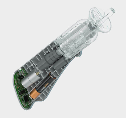
Altair solutions empower the design of electronic devices to meet structural and operational demands of normal use, drops, and misuse, while considering weight and cost. They enable simulation of structural, thermal, fluid properties, vibration, electromagnetics, and manufacturing constraints in an integrated multiphysics environment, ensuring robustness while optimizing performance and efficiency.
Delivering Functionality
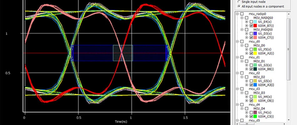

High-throughput Computing for Semiconductor Design
Delighting Customers
From Conceptual Design to Reality: Altair’s industrial design services can help customers with everything from user research to branding to design and prototyping. Altair® Inspire™ Studio software enhances creativity. Users can combine different modeling techniques to effortlessly create and explore even the most challenging designs.
Antenna Design and Placement: Altair® Feko®is widely used for the design of radio and TV, wireless, cellular, communication, remote keyless entry, tire pressure monitoring, satellite positioning, radars, RFID and other antennas. Feko’s Method of Moments (MoM) solver is used for antenna design. Model decomposition is possible with accelerated full-wave methods like Multi-level Fast Multipole Method (MLFMM), or asymptotic methods like Physical Optics (PO), Ray Launching Geometrical Optics (RL-GO) or Uniform Theory of Diffraction (UTD).
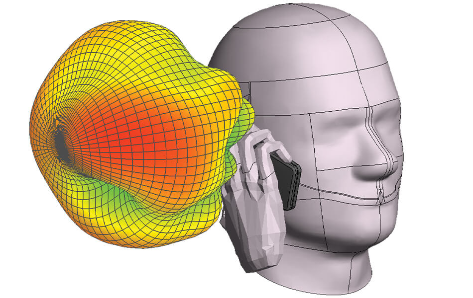
Device Compatibility: Electromagnetic compatibility (EMC) and electromagnetic interference (EMI) have become key topics with the proliferation of connected devices, both for component integration and satisfying EMC regulatory requirements. Feko can simulate both the radiation and irradiation of cables, antennas, and devices to inform the design of effective shielding. Feko also provides insight into the interactions of electromagnetic fields close to the body, ensuring safety while enough signal is radiated.

Guide to Electronic System Development
In today’s competitive landscape, manufacturers face the challenge of rapidly designing smart, interconnected products to stay ahead. With increasing performance demands and shrinking packaging sizes, collaboration between schematic engineers and product designers is crucial to optimize complex mechanical and electromagnetic systems efficiently. To drive efficiency and enhance device performance, companies are turning to simulation to create the next generation of smart products, enabling better decision-making and innovation.

Guide to Smart Product Development
The advent of the Internet of Things (IoT) has revolutionized business operations, offering avenues for unused product lines, recurring revenue streams, enhanced efficiency, improved quality, and faster time-to-market. Smart interconnections between systems and assets enable these benefits, allowing companies to realize their Smart Product Development vision seamlessly from ideation through optimization to launch and operation. This guide is designed to provide insights and support throughout the entire journey of Smart Product Development.

Consumer Electronics Design Guide
To guarantee the seamless delivery of a meticulously crafted electronic product to customers, the journey must initiate during the product design phase. Employing simulation-driven design, manufacturers gain profound understanding and authority over crafting innovative products, maintaining uniform manufacturing procedures, and adopting cost-effective, sustainable packaging solutions. This method enables manufacturers to fine-tune every facet of product development, ensuring top-notch quality and efficiency from inception to delivery.

Samsung Research Institute
The portable gadgets industry is fiercely competitive, pushing companies to constantly push the boundaries of their equipment design. With shorter design cycles and narrowing profit margins, there’s a greater emphasis on virtual testing using computer simulation. At Samsung Research Institute – Bangalore (the largest R&D center for Samsung devices outside Korea), Altair OptiStruct was utilized for shape and topology optimization to achieve a detailed definition of smartphone front and rear housing.